Chinese Startup Reports Photonic Chip Production Without ASML Lithography Machines
 1m, 28s
 2
2
13:24, 10.06.2026
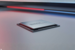
Chinese company Prinano has announced the successful production of 8-inch photonic chip wafers without using traditional deep ultraviolet (DUV) lithography equipment. The project was carried out in cooperation with Shenzhen Litra Technology.
With this move, Chinese companies aim to reduce their dependence on lithography equipment supplied by the Dutch company ASML, which is subject to export restrictions imposed by the United States and several other countries.
An Alternative to Expensive DUV Systems
Instead of conventional DUV lithography, the company employed its proprietary vacuum nanoimprint lithography (NIL) technology known as PL-AS. According to the developers, the new approach can reduce photonic chip production costs by approximately ten times compared to traditional manufacturing processes.
Unlike DUV or EUV lithography, where circuit patterns are transferred onto silicon wafers using light and optical systems, NIL technology works through physical imprinting. The PL-AS platform utilizes wafer-level pressure control, specially designed dual-layer imprint materials, and proprietary manufacturing processes.
According to Prinano, these technologies make it possible to create features smaller than 10 nanometers, bringing the platform closer to the requirements of modern semiconductor manufacturing.
A Technology With Great Potential and Challenges
Nanoimprint lithography has long been considered a promising alternative to traditional semiconductor manufacturing methods. It offers high precision while potentially reducing production costs significantly.
However, widespread adoption has been hindered for years by concerns related to defects, mold wear, throughput, and stable production yields. Because of these challenges, most chipmakers have continued to rely on established DUV and EUV technologies.
What It Means for the Market
If the claimed capabilities are validated in real-world production and successfully scaled for mass manufacturing, China could gain another tool for reducing its reliance on Western semiconductor equipment. At the same time, nanoimprint lithography could emerge as a lower-cost alternative for producing certain types of photonic and semiconductor chips.
Was this article helpful to you?
 Yes
Yes
 No
No
VPS popular offers
-10%


 Linux
Linux
€ 50 /mo
Billed annually
-20.2%
 Windows
€ 19 /mo
Billed annually
-10%
Windows
€ 19.99 /mo
Billed annually
-10%


€ 28.99 /mo
Billed annually
-15%
Windows
€ 101 /mo
Billed annually
-15.4%
Windows
€ 73 /mo
Billed annually
-10%
Windows
€ 28.44 /mo
Billed annually
-10%
Linux
€ 41.18 /mo
Billed annually
-4.7%
Windows
€ 10.57 /mo
Billed annually
-9.8%
Linux
€ 5.08 /mo
Billed annually