High-NA EUV Is Warming Up for Prime Time and Your Next Chip Will Feel It
 1m, 26s
 2
2
14:13, 17.02.2026
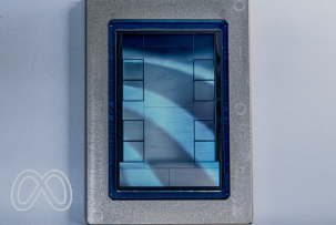
You are watching chipmaking approach a new cliff edge, and ASML wants to build the bridge. High-NA EUV lithography raises the numerical aperture to 0.55, which helps print far smaller features in fewer steps. In practical terms, this tool can form patterns down to about 8 nm in a single exposure. That capability points straight at 1.4 nm logic nodes and DRAM below 10 nm. The catch is cost. One High-NA EUV system can reach about $380 million, so every buyer must justify the math, not just the ambition.
Who Jumps First and Who Waits
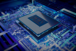
ASML expects Intel, Samsung, and SK hynix to lead the first real wave. Intel already brought an ASML Twinscan EXE:5200B online in December and links it to its Intel 14A roadmap. Samsung reportedly received its first EXE:5200B the same month and plans another delivery in the first half of this year, aiming to support future 2 nm-class production, including Exynos 2600 and potential contract work. SK hynix has worked with High-NA EUV since September and already uses standard EUV for DRAM. It plans multiple EUV layers in advanced memory. Meanwhile, TSMC appears cautious and does not plan to use High-NA EUV for its 1.4 nm node, likely due to economics. Micron still weighs timing, and Japan’s Rapidus eyes 1.4 nm production around 2029.
What This Means for You
You should expect High-NA EUV to reshape pricing and supply. Fewer patterning steps can improve yield, yet the tool’s price will pressure wafer costs at first. Over 2027 to 2028, broader adoption may bring more efficient production and new performance gains, but it can also deepen the gap between leaders and everyone else.
If this was useful, please share it with a colleague, and explore our other articles on chips, manufacturing, and the next node race.
Was this article helpful to you?
 Yes
Yes
 No
No
VPS popular offers
-8.9%


 Windows
€ 56 /mo
Billed annually
-10%
 Linux
Linux
€ 27.33 /mo
Billed annually
-9.7%
Windows
€ 138.99 /mo
Billed annually
-10%
Linux
€ 9.13 /mo
Billed annually
-10%
Linux
€ 135.49 /mo
Billed annually
-10%
Linux
€ 60.5 /mo
Billed annually
-10%
Windows
€ 18.1 /mo
Billed annually
-5.3%
Windows
€ 11.82 /mo
Billed annually
-9.9%
Linux
€ 5.05 /mo
Billed annually
-21%
Windows
€ 65 /mo
Billed annually