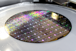
TSMC Completes Development of 1.6nm A16 Process
 49s
49s
 2
2
12:01, 21.08.2026

Taiwanese semiconductor giant TSMC has prepared its A16 (1.6nm) technology for mass production, successfully finishing its development and validation. The company's assembly lines are set to begin producing the first components using the new standard next quarter.
Super Power Rail Technology
The primary technological breakthrough of A16 is the transition to backside power delivery, which is TSMC's proprietary solution known as Super Power Rail (SPR). Combined with Gate-All-Around (GAA) transistors, the new process node will deliver an 8–10% performance increase at the same power consumption, or a 15–20% reduction in power consumption at equal frequencies, while increasing transistor density by nearly 10%.
A Stepping Stone to A14 and an Expanding Lead Over Rivals
Despite these impressive specifications, TSMC views A16 as a stepping stone toward the longer-lasting A14 process, which is scheduled for serial production in 2028. Nevertheless, the Taiwanese company remains significantly ahead of its competitors' roadmaps: Intel expects to begin mass production on its comparable 14A node no earlier than 2028, while Samsung plans to reach the SF1.4 standard only by 2029.
Was this article helpful to you?
 Yes
Yes
 No
No
VPS popular offers
-5%


 Windows
€ 12.1 /mo
Billed annually
-10%
Windows
€ 10.23 /mo
Billed annually
-7.2%
 Linux
Linux
€ 5.92 /mo
Billed annually
-21.4%
Windows
€ 67 /mo
Billed annually
-10%
Linux
€ 135.49 /mo
Billed annually
-10%
Linux
€ 49.99 /mo
Billed annually
-20.6%
Linux
€ 59 /mo
Billed annually
-24.7%
Linux
€ 31 /mo
Billed annually
-7.1%
Windows
€ 21 /mo
Billed annually
-29.4%
Linux
€ 17 /mo
Billed annually