Stacking the Future: 3D X-DRAM Steps Out of Theory
 1m, 19s
 2
2
13:51, 24.04.2026
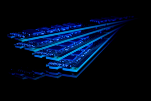
For years, engineers have dreamed of stacking DRAM cells vertically, similar to how 3D NAND transformed storage. That vision has now taken a real step forward. NEO Semiconductor has created a working silicon prototype of what it calls 3D X-DRAM.
This is not just another lab experiment. The company moved from struggling to attract attention to gaining serious interest from investors and industry players. Among them is Stan Shih, the founder of Acer and a key figure in semiconductor history. Partnerships with leading Taiwanese institutions helped turn this concept into reality.
Performance That Turns Heads
The prototype shows promising numbers. Read and write latency stays under 10 nanoseconds. Data retention exceeds one second even at high temperatures, which is far beyond current standards. Endurance also reaches impressive levels.
The architecture itself is what makes you pause. A massive data bus of about 32,000 bits and stacked memory layers could deliver up to 512 gigabits per chip. Bandwidth might surpass current HBM solutions by a factor of sixteen. That kind of leap could change everything from AI workloads to everyday computing.
What This Means for You
If this technology scales, you could see faster systems with more memory and lower costs. It may also reduce the gap between high-end and consumer hardware.
In our view, this is an early but meaningful signal. The memory industry rarely changes overnight, yet breakthroughs like this often define the next decade. If companies move quickly, you may feel the impact sooner than expected.
If you found this insight useful, share it with your network and explore more of our articles for deeper tech perspectives.
Was this article helpful to you?
 Yes
Yes
 No
No
VPS popular offers
-10%


 Windows
€ 18.65 /mo
Billed annually
-9.8%
 Linux
Linux
€ 5.08 /mo
Billed annually
-10%
Linux
€ 8.3 /mo
Billed annually
-10%
Linux
€ 69.99 /mo
Billed annually
-15.3%
Windows
€ 54 /mo
Billed annually
-15.4%
Windows
€ 73 /mo
Billed annually
-4.7%
Windows
€ 10.57 /mo
Billed annually
-10%
Linux
€ 9.19 /mo
Billed annually
-24.7%
Linux
€ 31 /mo
Billed annually
-10%
Linux
€ 26.35 /mo
Billed annually